Table of Contents
Executive Summary
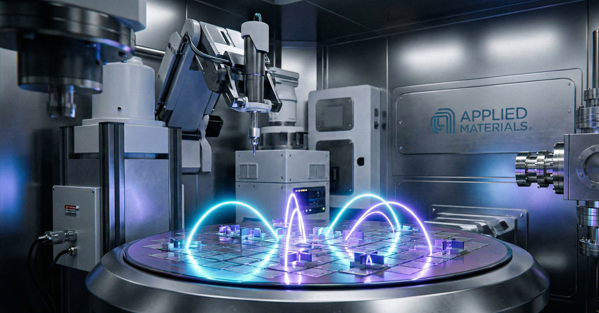
The global semiconductor industry has entered a transformative era defined by the rapid proliferation of Artificial Intelligence (AI) and the transition toward increasingly complex chip architectures. At the heart of this revolution lies Applied Materials, Inc. (NASDAQ: AMAT), a company that has redefined itself from a traditional equipment vendor to the foundational architect of the AI giga-cycle. This white paper explores the technological moat established by Applied Materials through its materials engineering leadership. It provides a granular comparison between AMAT and its primary peers, ASML Holding N.V. (NASDAQ: ASML) and Lam Research Corporation (NASDAQ: LRCX), and details how AMAT’s specific process tools are enabling the industry’s shift to 3nm, 2nm, and Gate-All-Around (GAA) transistors. For investors, understanding the interplay between materials science and chip performance is no longer optional; it is the key to identifying the long-term winners in a decade where hardware is the ultimate bottleneck for software ambitions.
The Renaissance of Materials Engineering in the AI Era
For decades, the semiconductor industry followed the predictable path of Moore’s Law, primarily driven by optical lithography—the ability to shrink features using light. However, as the industry pushes toward the 2nm node and beyond, the physical limits of materials have become the primary constraint. Shrinking a transistor is no longer enough; the industry must now change the very structure and composition of the materials used to build them. This shift has placed Applied Materials in a position of unprecedented influence.
Materials engineering is the science of manipulating matter at the atomic level to create new structures with specific electrical, thermal, and mechanical properties. In the AI era, where energy efficiency (performance-per-watt) is the most critical metric, the ability to engineer these materials is the industry’s “secret sauce.” Applied Materials’ moat is built on the broadest portfolio in the industry, spanning deposition, removal, modification, and analysis. While a competitor might dominate a single step of the manufacturing process, Applied Materials often owns the entire sequence of steps required to create a new transistor structure.
The PPACt Playbook: A Strategic Framework
Applied Materials operates under a strategic framework known as the PPACt playbook, which stands for Power, Performance, Area, Cost, and time-to-market. In the past, “Area” (scaling) was the dominant driver. Today, “Power” and “Performance” have taken center stage. AI workloads require massive data movement and computation, which generate immense heat and consume vast amounts of electricity. To solve this, chipmakers are moving away from traditional FinFET (Fin Field-Effect Transistor) designs toward GAA architectures. AMAT’s leadership in the materials required for these transitions—such as new metal gates, low-resistance contacts, and atomic-level smoothing—forms a barrier to entry that is nearly impossible for competitors to replicate without the same depth of integrated expertise.
Comparative Analysis: AMAT vs. ASML vs. Lam Research
To understand who wins the next decade, one must analyze the “Big Three” of semiconductor equipment. While often lumped together, their roles are distinct and increasingly complementary.
ASML: The Master of the Canvas
ASML Holding N.V. (NASDAQ: ASML) holds a monopoly on Extreme Ultraviolet (EUV) lithography. Without ASML, advanced logic and DRAM simply cannot be patterned. ASML is the company that “draws” the lines on the chip. However, lithography has become so expensive and complex that the industry is looking for ways to scale without relying solely on further lithographic shrinks. This is where “materials-enabled scaling” comes into play. While ASML remains a vital and dominant force, its growth is tied to the adoption of EUV and High-NA EUV. It is a “single-tool” powerhouse, whereas AMAT is a “multi-process” integrator.
Lam Research: The Specialist of the Vertical
Lam Research Corporation (NASDAQ: LRCX) is the leader in etch and deposition, with a particularly strong foothold in the memory market, especially 3D NAND. Lam’s tools are essential for creating the deep, vertical holes required in modern memory chips. However, Lam’s revenue is historically more cyclical due to its heavy exposure to the memory market. In the next decade, Lam is expanding its logic presence, but it faces stiff competition from AMAT in the transition to 3D logic structures and advanced packaging.
Applied Materials: The Integration Advantage
Applied Materials (NASDAQ: AMAT) distinguishes itself through breadth. It is the only company that can combine multiple process steps—such as epitaxy, ion implantation, and chemical mechanical polishing (CMP)—into a single vacuum environment. This is known as “Integrated Materials Solutions.” By processing a wafer through multiple steps without exposing it to the air, AMAT can create interfaces between materials that are cleaner and more efficient than those created by discrete tools from different vendors. This integration is the key to the next decade. As chips become 3D structures (GAA and 3D DRAM), the interaction between different manufacturing steps becomes more critical than the individual steps themselves.
Who Wins the Next Decade?
The winner of the next decade is the company that can best address the “energy crisis” of AI. While ASML will continue to be essential for the initial patterning, the heavy lifting of improving transistor performance and reducing power leakage will fall on Applied Materials. AMAT’s diversification across logic, foundry, and memory—combined with its leadership in the “ICAPS” (IoT, Communications, Automotive, Power, and Sensors) markets—gives it a more stable and broad-based growth trajectory. Investors often favor ASML for its monopoly, but AMAT’s “integration monopoly” in the materials space offers a comparable level of strategic importance with a wider addressable market.
Enabling Advanced Nodes: 3nm, 2nm, and GAA
The transition from FinFET to Gate-All-Around (GAA) nanosheets is the most significant architectural change in the semiconductor industry in over a decade. In a FinFET, the gate controls the channel on three sides. In GAA, the gate completely surrounds the channel, providing much better control over current flow and reducing power leakage. However, building a GAA transistor is an engineering nightmare that requires precisely what Applied Materials provides.
The Viva Pure Radical Treatment System
At the 2nm node, the silicon nanosheets must be perfectly smooth. Any atomic-level roughness on the surface of the nanosheet can impede the flow of electrons, leading to heat and reduced performance. Applied Materials introduced the Viva system, which uses a pure radical treatment to smoothen the surfaces of these nanosheets with atomic-level precision. This tool is not just an “extra” step; it is a requirement for the 2nm node to reach its theoretical performance gains.
Sym3 Z Magnum: High-Precision Etching
The vertical architecture of GAA requires carving deep, narrow trenches between the nanosheets. These trenches must be perfectly vertical and uniform across the entire wafer. The Sym3 Z Magnum etch system uses advanced pulsed voltage technology to control ions at a microsecond scale. This allows chipmakers to create the high-aspect-ratio features required for GAA without damaging the delicate underlying structures. This system has already seen broad adoption and is the “tool of record” for many 2nm logic manufacturing lines.
Spectral ALD and the Shift to Molybdenum
One of the biggest bottlenecks in modern chips is “contact resistance.” As transistors get smaller, the metal contacts that connect them to the rest of the chip become so thin that they struggle to conduct electricity efficiently. For decades, tungsten was the metal of choice. However, at the 2nm and angstrom nodes, tungsten becomes too resistive. Applied Materials is enabling a shift to Molybdenum using its Spectral Atomic Layer Deposition (ALD) system. Molybdenum can be deposited in thinner layers while maintaining superior conductivity, effectively “unclogging” the electrical pathways of the chip. This material innovation alone can provide a double-digit improvement in chip performance.
Advanced Packaging and Heterogeneous Integration
The AI era has also brought about the rise of “chiplets” and advanced packaging. Because it is becoming too expensive to put everything on a single massive chip, manufacturers are breaking chips into smaller pieces and “gluing” them together. This is Heterogeneous Integration. Applied Materials is a leader in the equipment needed for this process, particularly in Through-Silicon Vias (TSVs) and Hybrid Bonding. As AI chips like NVIDIA’s GPUs and specialized AI accelerators rely more on High Bandwidth Memory (HBM) stacked directly on the logic, AMAT’s packaging tools become as critical as its front-end manufacturing tools.
The Investment Perspective: Risks and Rewards
From an investment standpoint, Applied Materials offers a compelling combination of growth and resilience. However, the stock is not without risks.
The China Factor
Applied Materials has significant exposure to the Chinese market. Geopolitical tensions and export restrictions on advanced semiconductor equipment have created a headwind. While the company has successfully pivoted toward the “ICAPS” market in China—which involves less-advanced but high-volume chips for automotive and industrial use—any further escalation in trade wars remains a primary risk factor for the ticker symbol AMAT.
The Recurring Revenue Stream
Unlike many hardware companies, Applied Materials has a massive installed base of over 40,000 tools worldwide. This base generates high-margin recurring revenue through the “Applied Global Services” (AGS) division. As chip manufacturing becomes more complex, customers are increasingly relying on AMAT’s proprietary software and subscription-based service models to keep their fabs running at peak yield. This service revenue acts as a cushion during cyclical downturns in equipment spending.
Valuation and Market Leadership
In 2026, Applied Materials continues to trade at a premium relative to its historical averages, reflecting its central role in the AI build-out. However, compared to the valuations of AI software companies or even some fabless semiconductor firms, AMAT remains an attractively priced “picks and shovels” play. The company’s ability to return capital to shareholders through dividends and aggressive share buybacks further strengthens the bull case.
Conclusion
Applied Materials is no longer just a participant in the semiconductor industry; it is the enabler of its future. The move to 2nm and GAA architectures represents a “materials-first” era of computing where AMAT’s expertise is the primary lever for progress. While ASML provides the vision and Lam Research provides the verticality, Applied Materials provides the substance. Its leadership in materials engineering, combined with its strategic integration of process steps, has created a technological moat that is reinforced with every new node transition. For the next decade of AI-driven computing, the road to higher performance and lower power consumption runs directly through the tools and innovations of Applied Materials.