Table of Contents
Executive Summary: The Wide-Bandgap Imperative
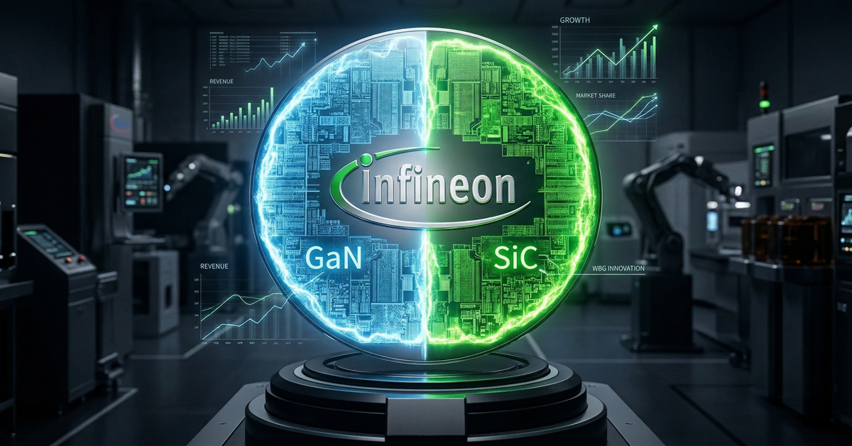
The global power semiconductor market is undergoing a structural paradigm shift. For decades, Silicon (Si) has been the undisputed foundation of power electronics. However, as global macro-trends—specifically the electrification of transport, the proliferation of renewable energy, and the exponential power demands of AI data centers—accelerate, traditional Silicon is reaching its theoretical physical limits. Enter Wide-Bandgap (WBG) materials: Silicon Carbide (SiC) and Gallium Nitride (GaN).
Infineon Technologies AG (XETRA: IFX) currently commands the largest share of the broader power semiconductor market. Yet, in the high-stakes sub-sector of SiC, the company has historically faced fierce early competition from peers like STMicroelectronics and ON Semiconductor. To secure long-term dominance, Infineon has laid out a highly aggressive, capital-intensive strategy known as the “30-30” goal: capturing a 30% global market share in Silicon Carbide by the year 2030, targeting annual SiC revenues exceeding €7 billion.
Achieving this objective requires flawless execution across three primary operational pillars: mastering the complex transition to 200mm SiC wafer manufacturing, leveraging a first-mover advantage in 300mm GaN production, and establishing absolute supply chain sovereignty in raw substrate procurement. This report provides a detailed, comparative analysis of these three pillars, evaluating their impact on Infineon’s cost-efficiency, margin expansion, and long-term equity valuation.
1. The 200mm SiC Watershed: Yields, Cost-Efficiency, and the Kulim-Villach Synergy
The transition from 150mm (6-inch) to 200mm (8-inch) SiC wafers is arguably the most critical operational hurdle in the WBG industry today. Silicon Carbide is notoriously difficult to manufacture; the material is nearly as hard as diamond and requires sublimation growth processes at temperatures exceeding 2500°C. Defect densities—such as basal plane dislocations and micropipes—historically plagued larger wafer diameters. However, the economic imperative to transition to 200mm is undeniable.
The Mathematics of Wafer Scaling and Yield
Moving from a 150mm to a 200mm diameter does not merely increase the total surface area by a factor of 1.77. Due to the geometric reality of semiconductor manufacturing, the “edge exclusion zone” (the perimeter of the wafer where dies cannot be reliably printed) consumes a disproportionately large percentage of smaller wafers.
We can model the usable area with the following equation, where is the wafer radius and is the edge exclusion margin:
Assuming a standard of 3mm, a 150mm wafer provides a usable area of approximately 16,286 square millimeters. A 200mm wafer provides roughly 29,559 square millimeters. Therefore, the actual usable silicon estate increases by more than 1.8x. When factoring in the rectangular geometry of power dies and the reduction of partial-die waste at the curvature, the actual die-per-wafer (DPW) yield can increase by 85% to 90%. This non-linear scaling drastically reduces the per-unit cost of SiC MOSFETs, providing a massive gross margin tailwind for the manufacturer that can successfully scale production.
The “One Virtual Fab” Strategy: Villach and Kulim
Infineon has fundamentally derisked this transition through its “One Virtual Fab” operating model, connecting its R&D and initial manufacturing hub in Villach, Austria, with its massive high-volume expansion in Kulim, Malaysia.
Villach acts as the vanguard. It is here that Infineon mastered the 200mm epitaxial growth and front-end device processing, successfully shipping its first commercial 200mm SiC products to customers in Q1 2025. By perfecting the recipe in Austria, Infineon drastically reduced the technology risk before porting the exact parameters to Kulim.
Kulim’s Module 3 represents a watershed moment for the industry. Backed by an additional €5 billion investment, this facility is engineered to be the world’s largest 200mm SiC power fab. By sharing identical processes, equipment software, and metrology standards with Villach, Kulim bypassed the traditional multi-year yield learning curve. The cost-efficiency generated here is unparalleled. While competitors like Wolfspeed have struggled publicly with the ramp-up of their 200mm Mohawk Valley facility due to isolated equipment optimization issues, Infineon’s dual-site redundancy ensures that yield improvements in Austria immediately translate to lower unit economics in Malaysia.
Furthermore, the Kulim expansion is heavily subsidized by the customer base itself. Infineon has secured approximately €1 billion in prepayments from major OEMs (including Ford, SAIC, Chery, and SolarEdge) in exchange for capacity reservation agreements. This drastically improves the Return on Invested Capital (ROIC) and ensures that the massive depreciation expenses associated with the €5 billion CapEx are immediately offset by guaranteed utilization rates, protecting Infineon’s consolidated gross margins.
2. 300mm GaN: The Next Frontier and the First-Mover Advantage
While SiC dominates high-voltage applications (typically 800V to 1200V) such as EV traction inverters, Gallium Nitride (GaN) is the undisputed champion of high-frequency, medium-voltage applications (100V to 650V). The GaN market for power applications is compounding at a remarkable 36% annual growth rate, projected to reach roughly $2.5 billion by 2030.
Overcoming the Physics of 300mm GaN
Historically, GaN has been grown on Sapphire or Silicon substrates. GaN-on-Silicon is the preferred method for power electronics due to the potential to leverage legacy Silicon manufacturing equipment. However, transitioning from 200mm to 300mm (12-inch) GaN-on-Si wafers introduces severe physical constraints.
There is a significant lattice mismatch and coefficient of thermal expansion (CTE) differential between the GaN epitaxial layer and the underlying Silicon substrate. During the cooling phase of manufacturing, this mismatch generates immense mechanical stress. As Infineon engineers have noted, the stress on a 300mm GaN-on-Si wafer is equivalent to the weight of four mature elephants concentrated on a single coin. If not perfectly managed through complex strain-relief buffer layers, the wafer will bow, warp, or shatter entirely.
Infineon achieved a massive technological breakthrough in late 2024 by successfully piloting 300mm GaN manufacturing in Villach, and they are on track to ship commercial customer samples by Q4 2025.
The Financial Impact of the First-Mover Advantage
The economics of 300mm manufacturing are transformational. A 300mm wafer holds 2.25 times the surface area of a 200mm wafer. Because the edge exclusion penalty is even further minimized, a 300mm wafer yields roughly 2.3x more functional chips per wafer pass.
This leads directly to the holy grail of the WBG industry: cost parity with Silicon. We evaluate cost parity at the level (the on-state resistance of the transistor).
By achieving this parity, Infineon eliminates the primary barrier to GaN adoption—price. This allows GaN to rapidly cannibalize traditional Silicon Superjunction MOSFETs.
This first-mover advantage is compounded by shifting competitive dynamics. In 2024/2025, TSMC, the world’s largest foundry, signaled a strategic retreat from GaN manufacturing to concentrate its capital on highly lucrative, leading-edge logic processors for AI. This exit created a massive supply vacuum. As an Integrated Device Manufacturer (IDM), Infineon owns its entire supply chain from epitaxy to packaging. By integrating 300mm GaN into its fully depreciated 300mm Silicon fabrication lines in Villach, Infineon requires minimal net-new CapEx to scale its GaN output, providing an insurmountable cost advantage over fabless GaN startups that rely on external foundries.
The margin implications are profoundly positive. High-density GaN power stages are becoming mandatory for AI data centers. As server racks transition from 12V to 48V bus architectures to support next-generation GPUs, power efficiency becomes a critical bottleneck. Infineon’s 300mm GaN devices will supply these high-margin enterprise applications, while the sheer volume of 300mm output will allow them to dominate the lower-margin, high-volume consumer electronics market (e.g., fast chargers and adapters) without eroding corporate profitability.
3. Supply Chain Sovereignty: Mitigating Geopolitical Risk via Multi-Sourcing
The greatest existential threat to any WBG semiconductor manufacturer is not demand-side adoption, but supply-side constraint. Silicon Carbide boules (the raw cylindrical crystals from which wafers are sliced) are the industry’s most critical bottleneck. Historically, substrate costs have accounted for an exorbitant 30% to 40% of the final SiC device cost. Furthermore, the global supply of high-quality SiC boules was previously monopolized by a handful of Western companies.
The Multi-Sourcing Strategy
Recognizing that relying on a single vendor or a single geographic region is unacceptable in today’s fractured geopolitical landscape, Infineon has ruthlessly executed a “multi-supplier and multi-country sourcing strategy.”
Instead of vertically integrating raw boule production (a highly capital-intensive and specialized chemical process), Infineon utilizes long-term agreements (LTAs) to pit suppliers against one another, ensuring competitive pricing and redundant supply lines. Infineon has secured extensive supply agreements with globally distributed partners:
- China: SICC and TanKeBlue (Securing massive capacity and insulating against potential trade embargos, allowing Infineon to serve the booming Chinese EV market with locally sourced substrates).
- Japan: Resonac (formerly Showa Denko).
- United States: Wolfspeed.
By heavily integrating Chinese suppliers SICC and TanKeBlue for both 150mm and emerging 200mm substrates, Infineon drastically reduces its exposure to Western-centric supply shocks. This is a masterstroke in supply chain sovereignty. If transatlantic trade tensions escalate, or if a specific supplier suffers a facility fire or yield collapse, Infineon’s production lines in Villach and Kulim will remain entirely uninterrupted.
Cold Split Technology: Maximizing Raw Material
Securing the boules is only half the battle; maximizing their utility is the other. Traditionally, SiC boules are sliced into wafers using diamond wire saws. Because SiC is incredibly hard, the sawing process takes hours per wafer and results in massive “kerf loss” (the material ground into dust by the saw blade). Often, up to 50% of the precious SiC boule is entirely wasted as dust.
To combat this, Infineon utilizes proprietary “Cold Split” technology. This process uses laser conditioning to create a micro-crack plane within the boule, allowing a perfect 350 thick wafer to be cleaved off mechanically, with practically zero kerf loss.
By driving to near zero, Infineon essentially doubles the number of wafers it can extract from a single purchased boule. When combined with the multi-sourcing strategy, Cold Split technology gives Infineon unparalleled control over its raw material costs, insulating its gross margins from the volatile spot market pricing of SiC substrates.
4. Investment Conclusion and Financial Outlook
Infineon’s roadmap to 2030 is arguably the most derisked and technologically sound strategy in the global power semiconductor space. The “30-30” goal is not merely an aspirational marketing slogan; it is backed by concrete operational physics and aggressive capital deployment.
The successful ramp of 200mm SiC in Kulim, utilizing the “One Virtual Fab” blueprint established in Villach, guarantees that Infineon will have the highest-volume, lowest-cost SiC capacity in the market. Simultaneously, pioneering the 300mm GaN frontier establishes an unassailable moat against fabless competitors, positioning Infineon to capture outsized margins in the booming AI data center and renewable energy infrastructure sectors.
Underpinning these technological achievements is a pragmatic, geopolitically agnostic supply chain strategy. By multi-sourcing boules globally and maximizing yield via Cold Split technology, Infineon has neutralized the primary risks that threaten its peers.
For institutional investors, Infineon (XETRA: IFX) represents a premier vehicle to capture the alpha generated by global decarbonization and digitalization. As the company crosses the 200mm SiC and 300mm GaN inflection points between 2025 and 2027, we project sustained gross margin expansion and a corresponding upward re-rating of the equity’s multiple, solidifying Infineon’s position as the undisputed sovereign of power systems.