Table of Contents
Executive Summary
As the artificial intelligence (AI) revolution transitions from a speculative hardware rush into a sustained infrastructure buildout, the focus is rapidly shifting from the digital processors (GPUs and AI accelerators) to the analog infrastructure that powers and tests them. Analog Devices, Inc. (NASDAQ: ADI) has quietly positioned itself as an indispensable architectural partner in this ecosystem. Recent financial results from early 2026 reveal a pivotal structural shift: ADI’s AI-related businesses—specifically its Automated Test Equipment (ATE) and Data Center Power and Optical solutions—now collectively account for nearly 20% of the company’s total revenue, representing an annualized run rate exceeding $2 billion.
This research report provides a comprehensive deep dive into how ADI is solving the two most critical bottlenecks in next-generation AI infrastructure: thermal management and power density. By delivering highly integrated power delivery networks (PDNs) that minimize energy loss and heat generation, and by providing the sophisticated ATE required to validate increasingly complex sub-5nm 3D-stacked chips, ADI is capturing unprecedented system-level content value. With its data center business growing at approximately 50% year-over-year and its ATE segment accelerating at 40%, ADI represents a compelling, highly profitable derivative play on the AI super-cycle, insulated from the fierce competition among digital chip designers.
The Macro View: The Power and Thermal Imperative in AI
The deployment of massive Large Language Models (LLMs) and deep learning networks has triggered an arms race in semiconductor performance. However, this performance comes at a steep physical cost. Traditional data center racks historically consumed between 10 to 15 kilowatts (kW) of power. Today, racks densely packed with advanced AI accelerators are pushing past 100 kW, with industry projections estimating rack power densities will approach 1 megawatt (MW) by 2028.
The Physics of Power Loss and Heat
At the silicon level, the latest generation of AI GPUs can individually draw upwards of 1,000 to 1,200 watts. Delivering this much power to a single piece of silicon at the ultra-low voltages required by modern logic (often below 1 volt) means delivering immense currents. According to Joule’s First Law, power loss in a conductor is proportional to the square of the current multiplied by the resistance:
When delivering over 1,000 amps of current, even a parasitic trace resistance of just 1 milliohm () on a printed circuit board (PCB) will result in a staggering 1,000 watts of wasted heat simply pushing the power to the processor ().
This wasted heat exacerbates the existing thermal challenges of the GPU itself. Modern 3D-stacked architectures, where high-bandwidth memory (HBM) is placed directly adjacent to or on top of logic dies, exhibit extreme localized heat fluxes ranging from to over . If junction temperatures exceed safe operating limits (typically around 85°C to 100°C), the silicon will dynamically throttle its clock speeds, destroying the expensive compute performance the data center operator paid for.
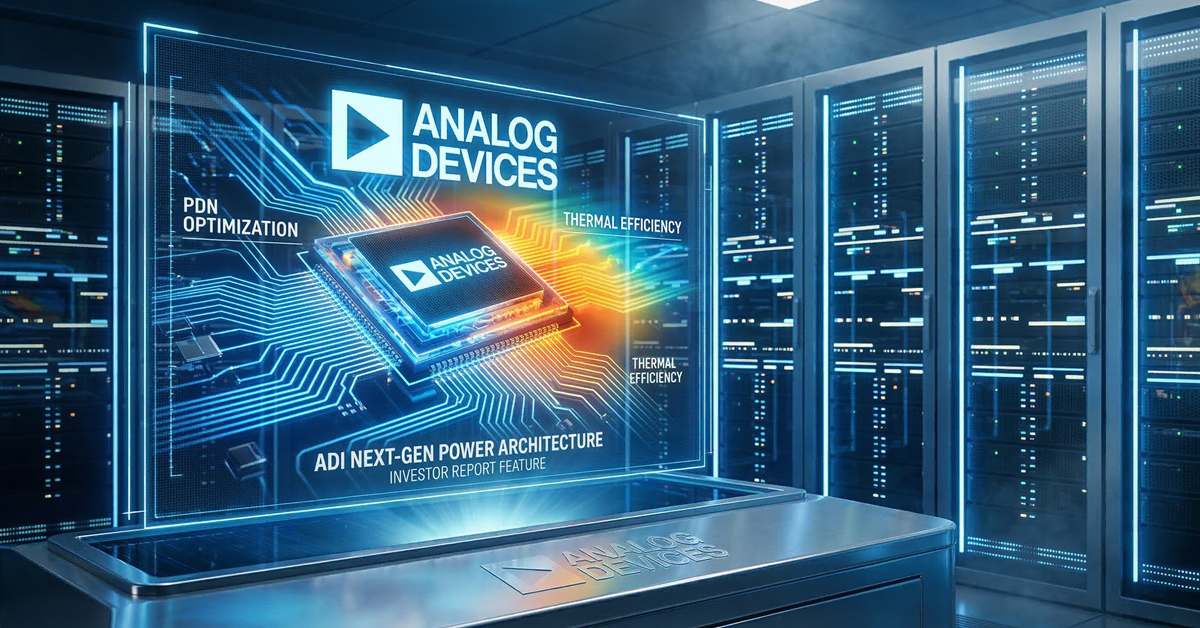
Therefore, thermal management in AI data centers is no longer just about liquid cooling or massive fans; it fundamentally begins with high-efficiency, localized power delivery. This is precisely where Analog Devices dominates.
Segment Deep Dive: Data Center Power & Optical Solutions
ADI’s data center business is roughly split down the middle between power management and optical connectivity. In the power domain, ADI provides the “vascular system” and the “brain” of the AI rack, capturing roughly one-third of its data center power revenue from hot swap and protection circuits, and another third from DC power control, such as multi-phase controllers and smart power stages.
Vertical Power Delivery Networks (VPDN)
To combat the challenge, ADI has pioneered advanced Vertical Power Delivery Networks. In a traditional lateral power delivery setup, the voltage regulator module (VRM) is placed next to the processor on the same side of the PCB. The power must travel laterally across copper traces, encountering parasitic resistance and inductance along the way.
ADI’s μModule® power regulators enable a vertical delivery architecture. The regulators are placed on the exact opposite side of the PCB, directly underneath the AI processor. Utilizing a shared pin map via through-hole connections, the power travels vertically through the board. This reduces the physical distance the current must travel from several centimeters to mere millimeters, virtually eliminating parasitic resistance and drastically improving the transient response.
The thermal benefits of this approach are twofold:
- It eliminates the parasitic heat generated by trace resistance.
- It declutters the top side of the board, allowing for massive, unobstructed liquid cold plates or heat sinks to be mounted directly flush against the processor die.
Highly Integrated Multiphase Controllers and SilentMOS™
AI workloads are notoriously dynamic, characterized by massive, instantaneous spikes in power demand (transient loads) when a neural network processes a batch of data. ADI’s digitally controlled multiphase controllers act as the brain of the power system, rapidly switching phases to deliver stable core voltages.
Coupled with ADI’s SilentMOS™ technology and patented coupled inductors, these smart power stages offer:
- Near 0 ns dead times: Enabling ultra-fast switching frequencies up to 3 MHz.
- Reduced Footprint: Achieving 1.82x smaller magnetics, critical for the space-constrained real estate surrounding an AI accelerator.
- Advanced Packaging: Utilizing dual-side cooling architectures that allow heat to be pulled from both the top and bottom of the power integrated circuits (ICs), lowering the thermal resistance () and improving overall system reliability.
48V/54V Intermediate Bus Conversion
As rack power skyrockets, data centers are shifting from legacy 12V distribution architectures to 48V and 54V direct current (DC) distribution. Transmitting power across the rack at a higher voltage drastically reduces the required current for the same power load, exponentially decreasing losses in the thick busbars. ADI is seeing accelerating adoption of its intermediate bus converter modules, which safely and efficiently step down these higher rack voltages to the localized voltages needed by the multiphase controllers.
Optical Connectivity and Circuit Switches
Beyond power, the remaining portion of ADI’s data center growth is fueled by optics. AI clusters require tens of thousands of GPUs to act as a single supercomputer, necessitating massive east-west data traffic with near-zero latency. As optical interconnects move from 800G to 1.6T speeds, the optical transceivers themselves become major heat generators. ADI provides precision power management, monitoring, and electro-optical interface control to ensure these optical links operate flawlessly under tight thermal constraints. Furthermore, as data centers begin transitioning to fully Optical Circuit Switches (OCS), ADI’s precision alignment and monitoring ICs represent a sticky, high-margin content expansion.
Segment Deep Dive: Automated Test Equipment (ATE)
While data center power is the most visible beneficiary of the AI buildout, ADI’s Automated Test Equipment (ATE) segment is arguably its most dominant moat. ATE revenue surged approximately 40% in fiscal 2025 and accelerated further in early 2026. This segment provides the instrumentation, pin electronics, and measurement subsystems that the world’s leading test vendors use to validate semiconductor chips before they are shipped.
The Complexity Multiplier of AI Silicon
The manufacturing of AI accelerators involves the most complex semiconductor processes in human history. Foundries are utilizing ≤5 nm technology nodes, utilizing tens of billions of transistors, and packaging them in intricate 2.5D and 3D heterogeneous packages.
This complexity exponentially increases the cost of failure. If a defective HBM module or a flawed logic die is bonded into a final 3D package, the entire $30,000 to $40,000 assembly must be discarded. Consequently, semiconductor manufacturers are dramatically increasing their test intensity at every stage:
- Wafer Probe Testing: Verifying known good dies (KGD) before packaging.
- Package/Final Testing: Verifying power-on functionality, standby leakage, and high-speed input/output integrity.
- System-Level Testing (SLT) and Burn-in: Running actual AI workloads on the chip in thermal chambers to stress-test the silicon and catch early-life failures.
ADI’s Value Proposition in ATE
ADI’s components sit at the absolute heart of these multi-million-dollar test systems. Management notes that ADI’s content per tester measures in the “tens of thousands of dollars.”
Testing sub-5nm chips requires instruments with picosecond jitter measurement capabilities and sub-10 noise floors. ADI’s ultra-precision analog-to-digital converters (ADCs), digital-to-analog converters (DACs), and highly integrated pin electronics deliver this exactitude.
Furthermore, as AI chips push the boundaries of power consumption, the ATE systems themselves require massive, highly controlled power delivery to stimulate the chip during a test. ADI’s power management IP is heavily leveraged within the test heads to deliver hundreds of amps of clean, transient-free power to the device under test (DUT). As the broader ATE market is projected to expand from $9.83 billion in 2026 to $13.67 billion by 2031, ADI’s high-end exposure to the fastest-growing sub-segments guarantees a long runway of secular growth.
Financial Performance and Valuation Analysis
Analog Devices has proven its ability to translate technical leadership into elite financial performance. The company’s Q1 FY2026 results established a definitive breakout from the broader semiconductor inventory correction that plagued the industry in 2024 and 2025.
Exceptional Top-Line and Margin Trajectory
- Revenue Reacceleration: Q1 FY2026 revenue printed at $3.16 billion, representing a 3% sequential increase and a robust 30% year-over-year growth, effectively exiting the cyclical trough.
- Gross Margin Durability: Non-GAAP gross margins hit 71.2%, up 240 basis points year-over-year. This was driven by higher factory utilization, a structurally favorable product mix shifting toward high-margin AI and industrial applications, and disciplined pricing actions reflecting the innovation premium of their long-lifecycle portfolios.
- Operating Leverage: Non-GAAP operating margins expanded to an exceptional 45.5% (up 500 basis points year-over-year). Adjusted EPS grew 51% year-over-year to $2.46.
Q2 FY2026 Outlook and Shareholder Returns
Management’s forward guidance is aggressively bullish, projecting Q2 revenue of $3.5 billion. This implies an 11% sequential growth rate—more than double the historical seasonal average of 4% to 5%. Importantly, the industrial segment (which houses ATE) is forecasted to grow 20% sequentially and 50% year-over-year, confirming that the upswing is driven by genuine end-market demand and not mere channel restocking. Operating margins are guided to expand further to 47.5%.
ADI is a cash-generation machine, producing $4.6 billion in free cash flow (39% free cash flow margin) over the trailing twelve months. Underscoring management’s confidence in the durability of this growth cycle, the company recently announced an 11% increase to its quarterly dividend (extending a 22-year streak of higher payouts), yielding approximately 1.27% alongside a highly active share repurchase program.
Valuation Assessment
Currently trading around $315 – $320 per share (a market capitalization of ~$155 billion), ADI carries a normalized forward Price-to-Earnings (P/E) multiple of roughly 36x. While this represents a premium to historical averages (typically hovering around 25x to 28x), the premium is thoroughly justified by the structural transformation of its earnings base.
The market has historically priced ADI as a cyclical industrial and automotive supplier. However, with AI infrastructure (Data Center and ATE) now commanding a $2 billion+ run rate and compounding at 40% to 50% annually, ADI is undergoing a multiple expansion event. The company is transitioning into a secular growth compounder. Peer comparisons show ADI’s return on equity and free cash flow generation easily outpacing broad-based competitors, making it a “quality-growth” anchor for any semiconductor portfolio.
Key Risks and Mitigants
No investment is without risk, and investors must monitor several key variables when assessing ADI’s medium-term trajectory.
1. Capital Expenditure Concentration Risk
The AI infrastructure boom is heavily concentrated among a handful of hyperscale cloud service providers. If these entities determine that their return on invested capital (ROIC) for AI software is not materializing, they could drastically slash their hardware capital expenditures.
Mitigant: ADI’s solutions are agnostic to which AI processor wins (Nvidia, AMD, or custom ASICs). Furthermore, ADI’s non-AI industrial and automotive businesses (which still account for over 70% of revenue) are in the early innings of a cyclical recovery, providing a revenue floor if AI CAPEX decelerates.
2. Geopolitical and Supply Chain Shocks
The majority of advanced AI chips and ATE systems are manufactured and deployed in Asia. Geopolitical tensions could disrupt the supply chain, halting the delivery of the systems that ADI’s chips power.
Mitigant: ADI operates a highly diversified hybrid manufacturing model. They maintain significant internal fabrication capacity in the United States and Europe for their proprietary analog processes, insulating them from leading-edge foundry bottlenecks.
3. Transition to Optical and Silicon Photonics
As data centers attempt to reduce power consumption further, there is a long-term threat that traditional copper-based power delivery and electronic switching could be partially displaced by entirely new paradigms, such as integrated silicon photonics computing.
Mitigant: ADI is heavily investing in the optical control layer. They are actively acquiring and developing IP to ensure they supply the analog signal chains required to modulate and control future photonics networks.
Conclusion and Strategic Outlook
Analog Devices is executing a masterclass in technological positioning. By recognizing early that the exponential scaling of digital logic would inevitably collide with the immovable laws of analog physics—specifically thermal dissipation and power delivery—ADI engineered a portfolio that is now mission-critical to the AI revolution.
The company’s advanced Automated Test Equipment components ensure the viability of next-generation 3D-stacked silicon, while its Vertical Power Delivery Networks and multiphase controllers prevent multi-million-dollar AI racks from melting down. With robust top-line acceleration, gross margins cresting 71%, and an unwavering commitment to shareholder returns, ADI presents a unique investment profile: the explosive growth upside of AI, insulated by the deep competitive moats and recurring cash flows of high-performance analog engineering. For investors seeking durable, highly profitable exposure to the physical infrastructure of artificial intelligence, Analog Devices warrants a cornerstone allocation.