Table of Contents
Executive Summary
As of March 2026, the global semiconductor industry stands at a critical geopolitical and technological crossroads. Intel Corporation (NASDAQ: INTC) is currently executing the most ambitious corporate turnaround in the history of the silicon industry. This sweeping transformation, previously branded as IDM 2.0 and now functionally operating as Foundry 2.0, seeks to restore Intel to process leadership while simultaneously building a world-class, pure-play external foundry business from the ground up. Over the trailing twelve months, Intel has experienced a historic equity renaissance, driven by unprecedented capital injections from the United States government, strategic partnerships with ecosystem titans like NVIDIA, and the stabilization of its next-generation 18A process node.
However, the transition from an Integrated Device Manufacturer (IDM) to a merchant foundry competing directly with Taiwan Semiconductor Manufacturing Company (TSMC) is fraught with structural, cultural, and financial hurdles. While Intel has successfully initiated volume production of its 18A node, effectively catching up to TSMC’s N2 timeline, the financial realities of scaling this technology are weighing heavily on the company’s near-term profitability. This comprehensive institutional investor report evaluates four critical pillars of Intel’s ongoing pivot: the technological viability of the 18A node against TSMC’s 2nm process, the integrity and transparency of the Foundry 2.0 customer pipeline, the capital expenditure milestones required to become the world’s second-largest foundry by 2030, and a granular review of Intel’s trailing one-year financial performance.
1. The 18A Litmus Test: Analyzing the Leapfrog Strategy Against TSMC 2nm
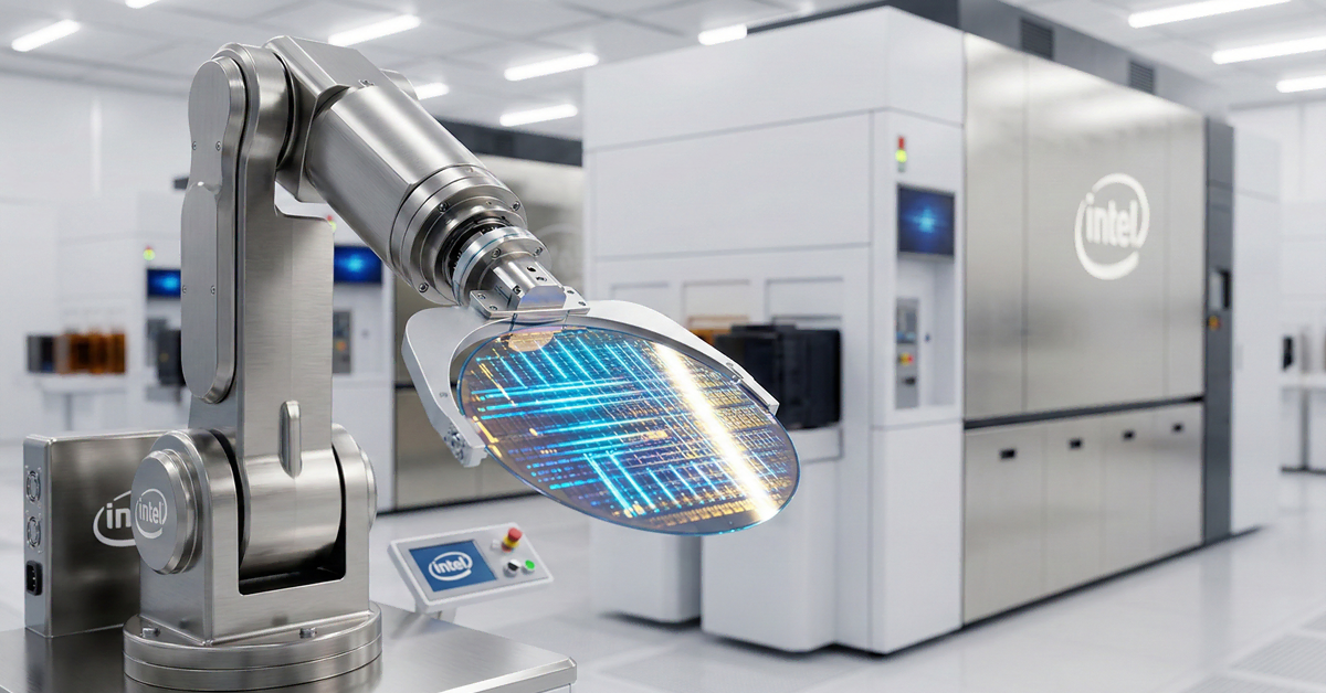
The core thesis of Intel’s entire foundry pivot hinges on the successful execution of its “Five Nodes in Four Years” strategy, culminating in the 18A (1.8-nanometer class) process. As of late 2025 and early 2026, Intel has officially commenced mass production of 18A, primarily serving its internal Panther Lake client compute tiles. Simultaneously, TSMC has quietly ramped volume production of its N2 node. The industry is closely monitoring whether Intel has truly leapfrogged TSMC, or merely closed a multi-year gap.
Transistor Architecture and Power Delivery Innovations
The technological battlefield at the 2nm tier revolves around two fundamental innovations: Gate-All-Around (GAA) transistors and backside power delivery networks. Intel’s implementation of GAA, branded as RibbonFET, replaces the legacy FinFET architecture. RibbonFET provides superior electrostatic control over the transistor channel, significantly reducing current leakage and enabling faster switching speeds at lower voltages. While TSMC is also debuting its own GAA technology (Nanosheet) with the N2 node, the true differentiation lies in power delivery.
Intel 18A represents the industry’s first concurrent implementation of GAA and backside power delivery, branded as PowerVia. In traditional chip design, power and data signaling are routed through a tangled web of microscopic metal wires on the front side of the silicon wafer. This creates severe routing congestion and voltage droop. By moving all power delivery to the back of the wafer, Intel clears the front side entirely for signal routing. This theoretically grants 18A a definitive advantage in power efficiency and clock frequency over TSMC’s baseline N2, which continues to rely on frontside power delivery (TSMC plans to introduce backside power with its N2P iteration in late 2026 or 2027).
Transistor Density and Silicon Economics
While Intel claims superiority in energy efficiency, TSMC maintains a formidable lead in raw transistor density. Density dictates how many transistors can be packed into a specific area, directly impacting the final cost per die. Industry consensus indicates that TSMC’s N2 achieves a high-density standard cell metric of approximately 313 million transistors per square millimeter. In contrast, Intel’s 18A achieves roughly 238 million transistors per square millimeter. For mobile chip designers like Apple or Qualcomm, where die area and cost are paramount, TSMC’s density advantage remains highly attractive. However, for high-performance computing and data center artificial intelligence applications, Intel’s PowerVia architecture offers thermal and voltage management benefits that may offset the lower baseline density.
Yield Curves and Defect Density
The ultimate arbiter of a node’s commercial viability is yield. A superior architecture is irrelevant if the foundry cannot produce functioning chips at scale. Throughout 2025, Intel aggressively drove down its defect density (D0) on the 18A node. Data from late 2025 indicates that 18A yields rose from roughly 50 percent to between 55 and 65 percent. While this is sufficient for Intel’s internal Panther Lake chips, which utilize smaller, modular chiplet architectures, it remains a precarious yield rate for massive, monolithic artificial intelligence accelerators. Furthermore, the physical process of manufacturing PowerVia requires grinding down the wafer and flipping it to construct the backside network, inherently adding complex, expensive steps that elevate the baseline manufacturing cost compared to TSMC’s N2. Intel must continue to rapidly mature its yield curve to drive down per-wafer costs.
2. Customer Pipeline Transparency: Evaluating the Foundry 2.0 Model
Technological parity is only half the battle. To justify the staggering capital expenditures associated with leading-edge fabs, Intel must attract massive volumes of external manufacturing orders. This requires convincing the world’s largest fabless chip designers to trust their most sensitive intellectual property to a company that, in many cases, is a direct competitor in the end-market. This operational framework is known as Foundry 2.0.
Constructing the Chinese Wall
The foundation of Intel’s external foundry pitch is the establishment of an impenetrable “Chinese Wall” between Intel Products (the chip design teams) and Intel Foundry Services. For decades, the Integrated Device Manufacturer model meant that Intel’s manufacturing arms existed solely to serve internal product roadmaps. Fabless giants feared that collaborating with Intel would inevitably lead to IP leakage. To rectify this, Intel has legally and financially separated the two entities. Intel Foundry now operates with a distinct enterprise resource planning system, isolated data centers, and rigorous legal frameworks ensuring that an engineer working on Intel Xeon processors has zero visibility into the foundry designs of external clients. Market confidence in this separation is the absolute prerequisite for long-term foundry success.
The Microsoft and Amazon Pipelines
The effectiveness of this Chinese Wall is being validated by early, high-profile adopters. Microsoft has emerged as the flagship external customer for Intel’s advanced nodes. Reports confirm that Microsoft plans to utilize Intel’s 18A and performance-enhanced 18A-P nodes to manufacture its next-generation custom silicon, specifically the Maia 2 artificial intelligence accelerators. This is a monumental endorsement. The Maia accelerators are massive, reticle-limit chips designed for intense cloud computing workloads. Microsoft’s willingness to bet its cloud infrastructure on 18A suggests deep confidence in Intel’s PowerVia technology and the maturity of its Process Design Kits.
Similarly, Amazon Web Services has partnered with Intel to produce custom artificial intelligence fabric chips. Both hyperscalers are motivated not only by technological merits but by supply chain resilience. Relying solely on TSMC presents severe geopolitical concentration risk. By cultivating Intel as a viable secondary source, Microsoft and Amazon ensure continuous supply even in the event of Pacific disruptions. However, it is crucial to note that these hyperscaler custom chips, while highly profitable on a per-unit basis, do not provide the sheer volume of wafers that mobile processors do. Intel’s pipeline still lacks a high-volume anchor tenant comparable to what Apple is for TSMC.
Financial Realities of the Foundry Pivot
Despite these strategic design wins, the financial translation of the Foundry 2.0 model remains painful. In the fourth quarter of 2025, Intel’s foundry business recorded an operating loss of 2.5 billion dollars against 4.5 billion dollars in revenue. Management openly acknowledged a cycle of heavy front-loaded investments paired with delayed demand realization. The broader Electronic Design Automation ecosystem is still actively catching up to Intel’s process rules. Synopsys and Cadence design flows are mature for TSMC, but optimizing them for Intel 18A remains an ongoing process. To secure sustainable profitability, Intel must seamlessly convert pilot programs and early test chips into sustained, high-volume mass production contracts by the end of 2026.
3. The Path to Number 2: Feasibility, CapEx, and Yield Milestones by 2027
Intel’s executive leadership has publicly established the goal of surpassing Samsung to become the world’s second-largest foundry by revenue by the year 2030. Achieving this target requires navigating a treacherous capital expenditure environment. The cost of advanced semiconductor manufacturing has spiraled exponentially, demanding strict financial discipline to avoid crushing the corporate balance sheet under the weight of factory depreciation.
Pivoting from Space to Tool Spending
An analysis of Intel’s capital expenditure strategy for 2026 reveals a fundamental shift. During the initial phases of the IDM 2.0 pivot, billions of dollars were poured into constructing concrete shells and massive cleanrooms in Arizona, Ohio, and Magdeburg. Entering 2026, Intel’s Chief Financial Officer David Zinsner confirmed that the company is dramatically scaling back spending on physical infrastructure. Having established a sufficient physical footprint, capital is now being aggressively redirected toward manufacturing equipment.
Intel has committed approximately 9.1 billion dollars strictly to tool spending in 2026. This capital is being deployed to equip existing cleanrooms with the lithography, etching, and deposition tools necessary to scale up 18A wafer starts. This pivot from “space” to “tool” spending is a positive indicator of capital efficiency, ensuring that dollars are directly tied to revenue-generating production capacity rather than dormant concrete facilities.
Gating the 14A Node and High-NA EUV
Perhaps the most critical display of newfound financial discipline relates to the upcoming 14A process node. Intel 14A will be the industry’s first node to widely deploy High-Numerical Aperture Extreme Ultraviolet lithography machines supplied by ASML. These tools cost hundreds of millions of dollars each and represent a massive escalation in capital intensity. Rather than preemptively building out massive 14A capacity under the assumption that demand will materialize, Intel management has stated that heavy 14A capital expenditures will be strictly gated. Investments will be limited to research and development until binding commitments and prepayments are secured from external foundry customers. This drastically reduces the risk of unutilized capacity and protects gross margins.
Yield and Utilization Milestones for 2027
To stay on the glide path toward becoming the second-largest foundry by 2030, several critical financial and operational milestones must be achieved by the close of 2027. First, factory utilization rates must reach approximately 80 percent. Semiconductor fabrication plants carry immense fixed depreciation costs; operating below 80 percent utilization typically results in severe margin compression. Second, 18A yields must stabilize in the high 80-percent range to match the unit economics of competing TSMC nodes. Finally, Intel must aggressively expand its advanced packaging capacity, specifically its Foveros and Embedded Multi-die Interconnect Bridge technologies. Advanced packaging has become the primary bottleneck in the AI accelerator market, and offering comprehensive packaging solutions is a mandatory prerequisite for capturing high-margin data center foundry contracts.
4. Evaluation of Intel 1-Year Trailing Performance (March 2025 – March 2026)
The financial performance of Intel Corporation from March 2025 through March 2026 has been characterized by explosive equity growth driven by strategic capital injections, followed by a harsh reality check as the fundamental costs of the turnaround materialized. Evaluating this trailing twelve-month period reveals a company that has successfully de-risked its balance sheet but is still battling immense operational headwinds.
The 2025 Equity Renaissance and Strategic Capital
Calendar year 2025 was a historic period for Intel’s stock, recording an 84 percent annual gain and significantly outperforming peers like NVIDIA and Advanced Micro Devices on a percentage growth basis. This massive rally was not fueled by organic cash flow, but rather by the successful execution of strategic funding initiatives that validated Intel’s geopolitical and technological importance. In August 2025, the U.S. government deployed an unprecedented 8.9 billion dollar direct equity investment, alongside nearly 7.86 billion dollars in CHIPS Act funding. This effectively provided a sovereign backstop to Intel’s capital expenditure roadmap.
Simultaneously, the private sector heavily endorsed Intel’s vision. Softbank injected 2 billion dollars into Intel to secure capacity and co-develop AI infrastructure. More surprisingly, NVIDIA committed a 5 billion dollar investment to jointly develop integrated CPU and GPU architectures, linking Intel’s x86 ecosystem with NVIDIA’s accelerated computing dominance. These capital inflows expanded Intel’s market capitalization to over 227 billion dollars by early 2026, signaling that the market viewed the bankruptcy or failure risk as effectively zero.
Earnings Volatility: The Q4 2025 Beat and Q1 2026 Guidance Drop
Fundamentally, the company showed brief flashes of operational momentum in the latter half of 2025. Fourth-quarter 2025 earnings beat analyst expectations, with revenue hitting 13.7 billion dollars. This was driven by earlier-than-expected traction in the AI PC market, specifically robust sales of the Panther Lake client processors. The ability to ship Panther Lake on the 18A node proved to Wall Street that Intel could execute advanced manufacturing at scale.
However, the euphoria was abruptly halted in early 2026. Following the strong Q4 report, Intel issued surprisingly weak guidance for the first quarter of 2026, projecting revenues between 11.7 and 12.7 billion dollars and a steep non-GAAP loss per share. This triggered a sharp double-digit stock decline in late January and early February 2026. The weak guidance laid bare the brutal economics of a foundry startup phase. The exorbitant depreciation expenses of the new Arizona factories, combined with high startup costs for the 18A node and underutilization of legacy nodes, continue to severely depress gross margins. Consequently, while the trailing one-year performance remains highly lucrative for investors who entered in early 2025, the stock is currently experiencing a turbulent consolidation phase as the market digests the long-term timeline required to reach sustained profitability.
In conclusion, Intel’s position in March 2026 is structurally sound but financially strained. The 18A node is a legitimate technological achievement, and the Foundry 2.0 customer pipeline is bearing fruit with hyperscalers like Microsoft and Amazon. However, the path to becoming the world’s second-largest foundry requires immense capital discipline, and the recent earnings volatility underscores that the financial turnaround will lag the technological turnaround by several years.