Table of Contents
Executive Summary
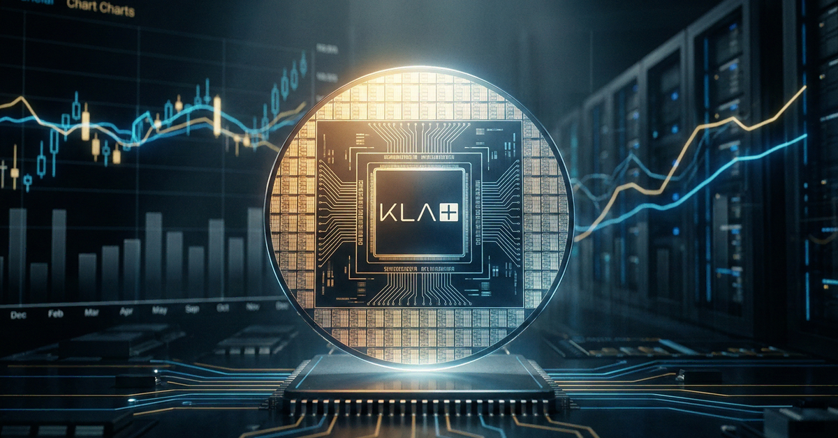
As of March 2026, KLA Corporation (NASDAQ: KLAC) stands at the absolute epicenter of the artificial intelligence infrastructure supercycle. While the market has rightfully fixated on the designers of AI accelerators and the foundries that manufacture them, the unsung beneficiary of this compute revolution is the semiconductor equipment sector—specifically, process control. KLA is the undisputed global leader in metrology and inspection, commanding an estimated market share exceeding 50% in this highly specialized niche.
This research report explores the structural catalysts driving KLA’s long-term valuation and revenue expansion. We are observing a paradigm shift in semiconductor manufacturing where the cost of failure has risen so astronomically that process control is no longer a secondary quality assurance step, but the primary enabler of fab economics. This shift is materializing across three distinct growth vectors: the rising process control intensity required for Gate-All-Around (GAA) transistors and 2-nanometer (N2) logic nodes; the explosive 70% year-over-year growth in KLA’s advanced packaging segment; and the hyper-complex yield dynamics of High Bandwidth Memory (HBM) required for AI GPUs. Despite near-term macroeconomic volatility and geopolitical headwinds, KLA’s robust capital return program, unyielding gross margins (historically >62%), and deep technological moats position it as a foundational asset for institutional exposure to the next decade of semiconductor advancement.
Introduction: The Economics of Process Control Intensity
To understand KLA’s strategic positioning, one must understand “process control intensity.” In the semiconductor capital equipment industry, Wafer Fab Equipment (WFE) spending is the total capital outlaid by foundries and memory makers to build out their manufacturing lines. Process control intensity refers to the percentage of that total WFE budget allocated strictly to inspection, metrology, and defect review tools.
Historically, as the industry progressed along Moore’s Law from 28nm to 14nm to 7nm, process control intensity hovered steadily around 10% to 12%. However, the transition into the angstrom era (such as TSMC’s N2 and A16 nodes, and Intel’s 18A) fundamentally breaks this historical baseline. When chipmakers utilize Extreme Ultraviolet (EUV) lithography and shift to 3D transistor architectures, the number of process steps per wafer increases exponentially. A modern leading-edge logic wafer can undergo more than 1,000 distinct manufacturing steps.
At a retail value of over $20,000 per leading-edge wafer, fabs simply cannot afford to wait until the end of the line to test for yield. If a systemic defect occurs at step 15, allowing that wafer to complete the remaining 985 steps is a catastrophic waste of time, chemicals, and opportunity cost. KLA’s equipment—ranging from broadband plasma (BBP) optical inspection to electron-beam (e-beam) review systems—is deployed directly inline. By catching defects at the atomic scale in real-time, KLA enables fabs to achieve profitable yield curves faster. Consequently, process control intensity is structurally rising, allowing KLA to outgrow the broader WFE market.
1. The AI Multiplier: Process Control at the Leading Edge
The buildout of global AI data centers is forcing a rapid acceleration in logic node roadmaps, directly benefiting KLA’s core systems business. As chip designers push the boundaries of physics to pack more compute density into AI accelerators, the foundries are retiring the standard FinFET transistor architecture in favor of Gate-All-Around (GAA) nanosheets.
The GAA Transistor Transition
In a GAA architecture, the transistor channel is entirely surrounded by the gate on all four sides, offering superior electrostatic control and preventing current leakage at microscopic scales. However, manufacturing GAA structures requires alternating epitaxial layers of silicon and silicon-germanium, followed by highly sensitive isotropic etching to release the nanosheets. This is a fragile, 3D mechanical structure that is highly susceptible to sub-nanometer defects, micro-voids, and critical dimension (CD) variations.
KLA is uniquely positioned to monetize this difficulty. The company’s highest-margin metrology tools are required to measure the thickness of these ultra-thin nanosheets, while its contamination control and overlay metrology tools ensure that successive layers align perfectly. According to TSMC’s aggressive 2026 capital expenditure budget of approximately $56 billion, roughly 70% to 80% is earmarked for the ramp-up of the 2-nanometer (N2) process and the ultra-advanced A16 node. Because N2 is fundamentally more complex to yield than 3nm, KLA captures more revenue per 100,000 wafer starts per month (WSPM) of capacity added at N2 than it did at previous nodes.
Actinic Reticle Inspection and High-NA EUV
Beyond the wafer itself, KLA is deeply entrenched in the photomask (reticle) ecosystem. The industry is currently transitioning to High-Numerical Aperture (High-NA) EUV lithography to print the smallest features of the N2 and sub-N2 nodes. A single High-NA EUV system from ASML costs upwards of $350 million. If the photomask used inside that machine contains a single defect, that defect will be perfectly printed onto every single die on the wafer, resulting in a 0% yield. KLA’s actinic reticle inspection tools utilize EUV wavelengths to inspect these masks before and during production, ensuring that multi-million-dollar production runs are not compromised. The AI buildout is directly funding the accelerated adoption of these ultra-premium logic nodes, cementing KLA’s tools as indispensable.
2. Advanced Packaging: The New Frontier of Revenue
Perhaps the most dramatic shift in KLA’s growth profile over the last 24 months has been the evolution of its advanced packaging segment. For decades, the semiconductor supply chain was neatly divided: “front-end” manufacturing happened in a cleanroom using advanced lithography to create the silicon dies, while “back-end” packaging was an outsourced, low-margin, commodity business involving plastic casing and wire bonding.
Advanced packaging has obliterated that distinction. Because it is no longer economically viable to build massive, monolithic silicon dies—due to the fact that larger dies inherently suffer from exponentially lower yield rates—the industry has embraced “chiplets.” AI processors, such as those from Nvidia and AMD, are no longer single chips. They are heterogeneous systems comprising multiple compute chiplets and memory stacks, all stitched together on a silicon interposer using technologies like TSMC’s CoWoS (Chip-on-Wafer-on-Substrate).
Shifting from “Back-End” to “Front-End-Like”
This paradigm shift has transformed packaging into a high-stakes, front-end-like process. Consider the economics: when a foundry is assembling a modern AI accelerator package, it is placing several “Known Good Dies” (KGD) onto an interposer. The combined value of these dies can easily exceed several thousand dollars. If the advanced packaging process fails—due to interposer warpage, a failed micro-bump, or a void in the hybrid bonding process—the foundry must scrap the entire assembly, destroying thousands of dollars of perfectly good silicon.
KLA’s Explosive Packaging Growth
To mitigate this exorbitant cost of failure, foundries are heavily inserting inspection and metrology tools into the packaging line. KLA is capitalizing on this trend massively. In calendar year 2025, KLA generated approximately $950 million in advanced packaging systems revenue, representing a staggering 70% year-over-year growth rate. Management has noted that their advanced packaging process control market share has surged from roughly 1% a few years ago to approaching 6% as of CY2025.
Looking into calendar 2026, the company expects this momentum to continue with year-over-year growth in the mid-to-high teens. The total advanced packaging market is currently valued at roughly $11 billion and is projected to reach approximately $12 billion in 2026, growing significantly faster than traditional core WFE. KLA’s Kronos and ICOS inspection platforms, designed specifically for heavy warpage handling, 3D topography, and fine-pitch substrate inspection, are becoming standard requirements for any facility attempting to manufacture AI accelerator packages.
3. High Bandwidth Memory (HBM) & The Memory Recovery
Artificial intelligence models are inherently memory-bound. While logic scaling has provided immense computational power, the speed at which data can be fed to the processor has lagged, creating the dreaded “memory wall.” The industry’s solution is High Bandwidth Memory (HBM), which physically stacks DRAM dies vertically to provide massive, parallel data lanes directly to the GPU.
The Mathematics of HBM Yield
HBM manufacturing is an extraordinarily delicate process. Current state-of-the-art AI accelerators utilize 8-hi (eight layers) or 12-hi (twelve layers) HBM stacks, with the industry aggressively moving toward 16-hi configurations. These dies are connected vertically using microscopic drilled holes called Through-Silicon Vias (TSVs) and copper micro-bumps.
The yield math for HBM exposes the critical necessity of KLA’s equipment. In a vertically stacked system, the failure of a single element compromises the entire stack. This relationship can be modeled probabilistically:
Where is the total yield of the HBM component, is the yield rate of the individual DRAM die, is the yield rate of the bonding process between layers, and is the number of stacked dies.
If a memory manufacturer attempts to build a 12-hi stack (), and their individual die yield is only 95%, the maximum possible yield of the stack before even accounting for bonding failures is , which equals an abysmal 54%. When factoring in bonding errors, the yield collapses further. Memory makers simply cannot achieve commercial profitability with a 50% scrap rate on premium memory components.
KLA’s Critical Differentiator
To drive and as close to 100% as physically possible, memory manufacturers like SK Hynix, Samsung, and Micron are aggressively purchasing KLA process control tools. KLA ensures that the TSVs are etched to the correct depth without cracking the silicon, that the micro-bumps are perfectly uniform in height to prevent open circuits, and that the DRAM dies themselves are free of yield-killing defects before stacking.
Furthermore, as DRAM architectures scale down, they require more logic-like processes, inherently increasing their process control intensity. KLA reported in its recent earnings that the memory segment now comprises approximately 40% of its semiconductor process control systems revenue, heavily weighted toward DRAM (roughly 85% of memory revenue) to support the explosive HBM capacity buildout. As long as the AI compute architecture requires massive parallel memory bandwidth, KLA’s memory segment will experience sustained, highly profitable growth.
Financial Performance and 2026 Outlook
KLA’s financial execution remains best-in-class within the semiconductor capital equipment sector. In its Q2 Fiscal Year 2026 earnings report (period ending December 31, 2025), the company demonstrated the profound operating leverage inherent in its business model.
- Revenue & Profitability: KLA reported quarterly revenue of $3.30 billion, surpassing the midpoint of its guidance, representing a 17% year-over-year increase. More impressively, non-GAAP diluted EPS reached $8.85. The company maintained its industry-leading non-GAAP gross margin of 62.6% and an operating margin of nearly 43%. This elite margin profile is a direct reflection of the proprietary value of KLA’s software, AI-driven data analytics, and the pricing power it commands as a near-monopoly in premium metrology.
- Cash Flow & Capital Returns: Free cash flow generation is a hallmark of KLA’s financial profile. The company generated a record $1.26 billion in free cash flow during the quarter, bringing its trailing twelve-month FCF margin to roughly 30%—placing KLA in the top 10% of all S&P 500 companies. This immense cash generation funds an aggressive capital return policy. Over the trailing 12 months, KLA returned approximately $3 billion to shareholders. Furthermore, management recently authorized a new $5 billion share repurchase program and raised the quarterly dividend by 12% to $1.90 per share, marking its 16th consecutive year of dividend growth.
- Recurring Service Revenue: A critical component of KLA’s margin resilience is its service business. In Q2 FY26, service revenue hit $786 million, up 18% year-over-year. Service contracts represent highly predictable, recurring revenue tied to the growing installed base of tools globally. As advanced nodes become more complex, fabs increasingly rely on KLA’s engineers and predictive maintenance software to ensure tool uptime.
- 2026 Market Forecast: Management projects the core WFE market to grow in the high single to low double digits in calendar 2026, reaching the low $120 billion range. Crucially, KLA expects to outgrow this broader market due to rising process control intensity. The company anticipates an acceleration in revenue growth in the second half of 2026 as new foundry capacity and broader AI investments come online.
Investment Risks and Competitive Headwinds
While the long-term thesis is robust, investors must contextualize the near-term risks and sector-wide volatility.
- AI Capital Expenditure Sustainability: Semiconductor stocks experienced broad selling pressure in early 2026 as markets questioned the sustainability of hyperscaler AI spending. If the return on investment (ROI) for massive AI data centers begins to lag, foundries may delay their equipment delivery schedules, which would immediately impact KLA’s deferred revenue and near-term cash flow.
- Geopolitical and Tariff Risks: KLA operates in a highly sensitive global supply chain. Historically, China represented a substantial portion of legacy node WFE spending. KLA management anticipates that due to ongoing U.S. export controls and normalization of buying patterns, China revenue will settle into the mid-20s percentage range of total revenue in 2026. Furthermore, the company noted that Trump-era tariff impacts are currently creating a roughly 100 basis point headwind on margins in the near term.
- Supply Chain Costs: Ironically, KLA is currently experiencing cost pressures from the very components its tools help manufacture. Management noted in Q3 FY26 guidance that rapidly escalating costs for the DRAM chips used inside KLA’s own image processing computers are creating a slight drag on gross margins, alongside extended lead times for certain components.
- Valuation: KLA’s stock trades at a premium. With a forward 12-month Price-to-Sales ratio above 13x and trading at higher forward earnings multiples than the broader market, the stock is priced for flawless execution. However, a Price-to-Earnings Growth (PEG) ratio near 1.8x suggests that the valuation remains justifiable given the structural earnings growth driven by AI.
Conclusion
KLA Corporation is not merely a participant in the semiconductor manufacturing ecosystem; it is the ultimate arbiter of yield. As the industry transitions to Gate-All-Around logic architectures, embraces heterogeneous advanced packaging, and scales vertical High Bandwidth Memory to feed data-hungry AI models, the complexities of chipmaking have outpaced the capabilities of traditional manufacturing lines.
Process control intensity is no longer discretionary. The exorbitant cost of failure at the angstrom level mandates the pervasive deployment of KLA’s optical and e-beam inspection platforms. Supported by an expanding, high-margin recurring service business, disciplined capital allocation, and >60% gross margins, KLA offers investors a fundamentally insulated, highly profitable vector into the artificial intelligence boom. For the institutional investor seeking structural semiconductor growth devoid of the binary risks associated with individual chip designers, KLA Corporation represents a premier, long-term capital compounding vehicle.